Welcome to the introductory page of the myCPU project. Free myCPU Introduction chapter from the myCPU Book Public repository of the myCPU Project
The myCPU is a fully modular 8-bit CPU. It was designed using only discrete logic components, and implemented with the most common integrated circuits from the 74 family. The myCPU project uses the Microprograming Technique to process instructions, relying on Microinstructions the instruction execution flow, and supporting the debugging at a microinstruction level. The myCPU was designed on printed circuit boards (PCBs), and it can built using TTL or CMOS technologies.
The feature of debugging at microinstruction level allows to observe the execution of individual microinstructions, stepping through each one and view the state of all logic components statically. This provides a detailed view of the instruction execution flow in real time.
A development and learning Platform
The myCPU was designed as a learning platform to provide an educational experience in the workings of a CPU, including the logic elements involved in its basic architecture and how several digital logic elements interact in a synchronized way.
With a modular design and hardware-level accessibility, myCPU serves as development platform. The myCPU platform enables the direct access to the relationship between hardware and software and give builders the opportunity to design their own modules. Thanks to the Instruction Decoder module, a programmable EEProm-based microinstruction decoder, builders can create their own instruction set for program writing.
The myCPU architecture was designed with the purpose to provide a clear understanding of a CPU system and its workings to people of all levels, including beginners. The design of myCPU architecture and modules is very simple and accessible to all levels, and the choice of components was made to provide an easy manipulation and a comfortable assembling experience. The components can be easily purchased from a variety of sources, including non-official online retailers and official stores.
You can see a more extensive explanation about the components in the dedicated page The Components.
The myCPU design was planned from the beginning as a learning platform. Even though its design could be improved for a better performance, that was not a primary objective in its develop. The main objective, as learnning platform, was the modularity, the open hardware architecture, the availability of components and ease of assembly, and the accesibility of the design to beginners, students and less experienced people.
The next list shows some of the topics you can learn with this project:
- Understanding the electronic relationship between software and hardware
- Understanding a basic CPU architecture, blocks, and logic devices involved
- Learn how a CPU execute an instruction and a whole program
- Learn how to implement a CPU instruction set and design new instructions
- Learn what a microinstruction is and how microinstructions are decoded
- Understanding the timings of a CPU, and the cycle of an instruction
- And much more.
In this introduction, we will cover aspects of the myCPU that might seem obvious to experienced individuals. However, as learning platform, it’s useful to review some topics to gain a deeper understanding of the design. In this way, we can appreciate how myCPU looks like a real CPU, rather than just seeing it as a simple electronics device.
The extensive documentation provided around the project may appear redundant or over-detailed to experienced individuals, but it is valuable for beginners or those with limited knowledge of digital electronics, who are taking his first steps in the knowledge of CPUs.
Open Architecture and modular design
The myCPU was designed with the open architecture concept in mind, focusing on modularity and ease of customization. Both features enable scalability in size and complexity by adding additional modules or replacement the provided ones with more advanced modules.\
This design was possible by the use of a base hardware layer composed by \textbf{chained BUS module boards}. The boards in the chain connect the data and control buses each other, and share them with the two modules plugged on both sides of the board. Each BUS module supplies power to the connected modules through its own voltage regulator and the 9V power source is shared along the chain. As a result, the power supply of a big modular circuit, like myCPU, could be possible successfully without any issues. Letting you increase the capabilities of myCPU by adding more BUS module boards and additional modules. Due to the basic nature of the first release of myCPU, just 8 BUS module boards are needed to built a basic myCPU layout, although up to 10 BUS module boards will be provided in the myCPU kit. Making it possible to build a chain of 8 BUS module boards in a vertical layout or 2 chains of 4 BUS module boards in a landscape layout to run the myCPU.
The modular and open architecture of the myCPU allows you to customize its functionality and behavior by designing your own modules and module boards
When designing custom modules, the only consideration to keep in mind, to maintain the compatibility with the myCPU design, is to properly place the control and data bus connectors according the mechanical dimensions specification of the BUS module board design.
You can check the mechanical dimensions in the technical documentation of the myCPU available at the Downloads page.
Custom modules, also can be designed using the protoboards provided in the kit, which was designed to be fully compatible with the BUS module board and will be provided in both side versions. See the section about Protoboards.
Moreover, the modular design allows you to customize the module layout of your myCPU by choosing your preferred module distribution. You can create different variants of module distributions, using either one chain of BUS module boards for a vertical myCPU layout or two chains connected by the myCPU layout connector for a landscape version. However, not all module distributions may be possible due to the flat wire connections between certain modules forming a block. In addition, the position of a module will also depend on whether it has versions for both orientations: left and right. Regardless these limitations, you will find that the platform is highly flexible.
Hardware architecture
The myCPU physical architecture consists of 3, vertically stacked, hardware layers, plus an additional optional layer if a module expansion board were used as part of a module.
- BUS layer (Main board layer providing power supply)
- Module layer (Modules)
- Auxiliary layer (Output display or auxiliary modules)
The concept behind this hardware architecture is separating BUS lines and power supply from the modules using a base BUS layer. This allow the buses to be shared among the module boards, through a base chain of BUS module boards composing the BUS Layer. The logic elements forming the CPU are implemented as separate modules on a Module layer and connected to the buses through the BUS layer. The output display functionality is also isolated from the modules through an Auxiliary layer.

The multiple layer characteristic enables the upgrade of the features of the myCPU by replacing existing modules with new ones without altering the existing BUS module base structure.
The Module layer enables the possibility to design logic devices in a independent way and connect them to the buses through the BUS layer. Additionally, it allows the development of complex logic devices and segmenting them into smaller components such modules, establishing connections between these module segments using direct flat wires and IDC connectors.
The Auxiliary layer enables to design your own display or output modules, separating the output from the module layer using an output connector. The myCPU kit includes three types of display modules: a 4-digit display for displaying an hexadecimal or decimal view of binary values, an 8-bit LED binary display using 3mm rounded LEDs, and an 8/16-bit binary display using LED bars for a clean visualization of a digital value.
Chained BUS module board design
The BUS module board was designed to connect multiple BUS module boards together to form a chained structure, which support the myCPU layout formed by the modules. This is achieved by using two female connectors at the top and two male connectors at the bottom of the board connecting the BUS module boards between them.

The myCPU supports different types of architectural layouts thanks to its modular nature. The most common are: Vertical and Landscape layouts but other layouts would be possible; In a landscape layout, 2 chains of BUS module boards are connected using the Layout Connector at the top, to share the buses between both chains, and the Layout Terminator at the bottom. In a vertical layout only a Single Layout Connector at the top is needed to provide the power source to the layout, and using IDC empty connectors such as terminators at the bottom to a clean isolation.


The data and control buses, as well as the 9V power source, are propagated from one BUS module board to the next BUS module board in the chain using the top and bottom connectors of the board. And the buses are shared with the modules through a connectors pair located on both sides (left and right) of the BUS module board, as you can see in the picture. For a more detailed explanation of the buses, see the section: The Buses.

Each Bus module board has its own +5V power supply using a 7805 voltage regulator, supplying power to the two modules plugged in to the board. The power source is supplied to the Bus module regulators through the chain connectors, and the +5v power is supplied to the modules through the Control BUS connector.
This approach enable the use of a common 9V power source to provide a stable +5V power supply to the pair of modules plugged in to each Bus module board, without any voltage drop or electrical issues. The Layout Connector module board has the power source connector, a power switch and filter capacitors providing a clean +9v power supply to the BUS module boards. You can find a full description of the BUS module in the related page: The BUS Module.
This design, makes it possible to increase the capabilities of the myCPU by adding more Bus module boards to the chain. This helps to avoid electrical issues, related to the power supply needs of the ICs in a TTL compatibility environment, that could arise due to the size of the myCPU circuit. Supporting the scalability of the myCPU with additional modules, more complex modules at double board size or even composed blocks of modules.
Functional architecture
The functional architecture describes the myCPU logic modules by their functionality, response to specific control signals and size of the data exchanged between each module with the data bus. In addition, the myCPU functional blocks showing the connections between modules belonging to a functional block. Figure bellow shows a diagram with a detailed view of the functional architecture.
The myCPU design is based on 16 functional modules distributed over 15 physical modules and 8 functional blocks.
You can download all myCPU diagrams from the Diagrams download page.
Figure below shows a diagram with a precise detail of the functional architecture.

A printable PDF version of the diagram: myCPU Modules Diagram
One of the most interesting features of the myCPU design, from a learning perspective, is that almost every logic element of the functional architecture corresponds to a physical module in the myCPU kit. Each module can be exchanged separately with new modules in an upgrade, or with custom modules with same behavior but different characteristics, a variation of its main digital functionality or simply changing the type or model of some of the logic components of the original module design.
Functional blocks
In the myCPU design, logic modules sometimes are grouped as “Functional Blocks” because they working together to perform a specific task and could be connected by a dedicated connection, as in the case of the ALU module with the accumulator and operand register modules, the SRAM module with the MAR module or the Instruction Decoder module with the Sequencer, Flags Register, Instruction Register and CSM modules.
The myCPU is based on 7 functional blocks, plus one Auxiliary block which includes the modules providing specific functionality or connectivity. Each block is composed by one or more functional modules and could be implemented using one or more physical modules. Bellow you can see a diagram of the functional blocks architecture:
Printable PDF version of the diagram: myCPU functional blocks Diagram


Modular architecture
The myCPU was designed with a modular implementation in mind, allowing the separation of functional logic over independent modules. This enables the design of modules focused on specific logical functions, and implementing them as standalone physical modules. A modular architecture allows builders to create their own custom modules, control their complexity, and even personalize functional blocks by blending their own custom modules with those included in the myCPU kit.
This myCPU feature is very interesting, because you can redesign some of the modules included in the kit with your own new or modified version, while leave the others without any changes. An existing module could be redesign entirely or just change one IC by another IC model, for example changing the pair of 4-bit D-Type register 74xx173 IC of the Accumulator module by only one 8-bit D-Type register 74xx377 IC.
Another benefit of a modular architecture is the possibility of creating modules using the protoboards provided in the myCPU kit, or any other physical base for the module implementation.
Modules have left-side or right-side compatibility, restricting their available positions on the BUS module board. \textbf{Right-Side} modules cannot be plugged into the left side and \textbf{Left-Side} modules cannot be plugged into the right side. Not all modules have been designed for both-side compatibility, at the moment of write the book only the general-purpose register ABC board has versions for both sides.
Thanks to the modular architecture, you can build a highly personalized myCPU layout with a module distribution according to your preferences.
The myCPU design allows to build customizable distributions of modules over the myCPU layout.
Module distribution layouts
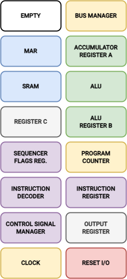
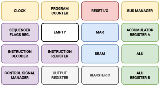
According to the BUS module design, and thanks to its modular architecture, you can choose the positions of the myCPU modules to configure the myCPU layout. You will have the ability to build different physical layouts by plugin the modules in different positions. This feature enables you to customize the layout of your myCPU to suit your preferences, to having a clean visualization of certain modules or get an ease of access to manipulation and testing. In my case, I prefer to place the clock module at the bottom of the layout, the BUS manager module at the top, and the memory block composed of the MAR and SRAM modules at the bottom as well, to make it easier to access the test switches.
The myCPU design has some layout limitations related to the modules belonging to a functional block and are interconnected between them, or related to the side version of the module. Modules belongs to a functional block may need to be placed together due to the wiring between them.
Beyond customizing the distribution of the modules over the myCPU layout, you can also choose between two architecture layouts: vertical or landscape. You can use a unique BUS module chain for the vertical layout or two BUS module chains for the landscape layout. The vertical layout need to be connected with Single Layout Connector to provide the power supply input and single IDC empty connectors at the bottom as terminators. The landscape layout should have the chains connected by the Layout Connector at the top, to provide the power supply input as well and the Layout Terminator at the bottom to keep electrically closed both chains , left and right. You can See more info about at the page about Layout Connectors.
At the beginning of the Open Architecture section you could see two images of real layouts.
Functional and physical Modules
The myCPU architecture design include 16 functional modules in the final release, implemented on 15 physical module boards because the sequencer and the Flags register were designed on the same physical module board. Below you can find a list with all module boards will be provided in the myCPU kit.

Navigate to Introduction page of modules for more information related to the myCPU modules and the module design in the open architecture.
Display Modules
The myCPU design include, display functionality is isolated from modules using general purpose output connectors, like output ports, forming the \textbf{Auxiliary Hardware Layer}. Output data from the module are shared through output connectors. In the myCPU final release, there’s will be 3 types of display modules: two of them are LED based binary displays and the other is a 4 digits binary to hexadecimal/decimal decoder display. The 8 bits LED displays use 3mm rounded LEDs and the 16 bits displays use 8 segments LED Bars for a better visualization. Displays can be plugged in all modules with and available output connector, but 4 digits displays only are supported by modules with enough space to hold the display. Whenever be possible, I recommended to use the 16 bits LED Bar display instead a rounded 8 bits display for a flat and clear binary value visualization.

You can see a better description of each extra module on related Display pages at modules menu.
Additional tools and extra boards
The myCPU kit includes one utility board to build a programmer for the AT28C64B EEproms used in the myCPU. It includes two auxiliary boards to connect and power the myCPU layout chains mentioned earlier in the section “Chained BUS module board design”. Also, it includes two extra board types for prototyping: A simple protoboard for general purpose and a specified protoboard with built-in support for data BUS output using a 74xx245 and an output port added to the board. The protoboards provided have compatibility for left and right sides.

You can see a better description of each module on the related pages at the Extra modules menu:
Features of myCPU
In the next table you can find a brief list of myCPU digital features. Some of these features come from the original design of the Ben Eater’s breadbooard computer and others are improvements over his design. It is highly recommended to understand the meaning of these features in relation to the design of the myCPU. In the following sections, I will briefly explain what each of those features means.

The Buses
The myCPU uses only two buses to facilitate data and control signals sharing, and connectivity between modules: the Control Bus and the Data Bus. The myCPU design follows the “Von Neumann Bus Architecture”, where data and memory addresses are shared over the same bus, being the Data BUS in the myCPU design. Despite the myCPU basic design, is important for students or beginners to take note of this particular aspect of the myCPU. Something like a dedicated Address Bus is only present in the connection between the MAR and SRAM modules.
The Data Bus supports data lengths up to 16 bits, which will be enough for future releases of the myCPU using the same BUS module board design, and should be enough to design custom modules or modules prototypes handle more than 8 bits. With 16 bits, we can share values such as addresses up to 64Kb, which satisfies the requirements of a very basic CPU like myCPU, and a more complex cpu in the future.
Due to the 8-bit nature of the myCPU, could be enough to use only 8 bits for data exchange. However, this may result a limitation by the need of multiple fetch cycles to manage 16 bits of data. The Management of 16 bits of data using 8 bits of data transfer requires at least 2 clock cycles for each exchange of data between registers and memory, so a 16 bits Data BUS is a very interesting feature for a learning platform like the myCPU, and is a essential feature for future releases like the the myCPU2K and beyond.
All of the myCPU control signals are transmitted through the Control Bus. The Control Bus has a capacity of 32 lines via a 32-pin connector, although not all of these lines are used for control signals. The voltage regulators, located in each bus module board, uses the GND and +5v pins of the Control Bus to provide power to the modules. The clock and reset signals, as well as the status flags signals, also travel through the Control Bus.
The lines included on the control BUS are distributed as indicated in the list below:

The Control Signals of myCPU
The myCPU support up to 23 control signals to drive the logic devices of myCPU. 22 of the control signals are managed directly by a dedicated module: the \textbf{Control Signals Manager (CSM)}, which sets the corresponding digital state for the control signals sent to each logical device in the myCPU. But there’s and exception, the \textbf{SQR} control signal is internal an handled directly by the Instruction Decoder to control the instruction cycle length.
More info about control signals can be found at the CSM module page.
The below table shows the full list of the myCPU control signals describing the action produced on the modules.

Knowing the default values of each control signal is essential for a proper understanding of the behavior of the modules. In the myCPU platform, Control signals are the truly key in the interaction between the hardware (modules) and the software (instructions). The myCPU is based on microprogramming, so instructions are composed by microinstructions, those microinstructions are binary strings composed by control signals acting directly, trough the CSM module, on the electronics of the modules modifying their behavior or logic state.

Designing your own custom modules will require a deep understanding of the control signals, their default values and the actions they produce on the logic components of the modules.
Signed display mode support
The myCPU support a 2’s complement display mode, affecting basically, to the mode on how the hex/dec decoder display shows binary values, not to the manipulation of a binary value itself. There’s a control signal UN which enable the 2’s complement display mode.
When the UN control signal is LOW, decimal displays show numbers as unsigned, with a range from \textbf{0 to 255}. When the UN control signal goes HIGH, decimal displays show numbers as signed, using 2’s complement representation with a range of -128 to 127. This feature is in line with the corresponding feature of the output module in the Ben Eater’s project.
You should watch the Ben Eater’s video about: Two’s complement arithmetic
The Instruction Cycle
The myCPU instruction execution is performed through an Instruction cycle that composed by a Fetch cycle followed by an Execution cycle. The myCPU is based on single fetch execution cycle, it means that uses only one fetch cycle to get the instruction and the argument of the instruction. This is possible thanks to an Instruction Register with a 4+4 bits design, using the most significative 4 bits for the OpCode of the instruction and the less significative 4 bits for the argument. So, in a single 8 bits data exchange operation with memory are retrieved the instruction plus the argument, being the most simplified way to view and understand the execution cycle of a CPU in real time.
Due to the simplicity of the myCPU instruction set and the programming limitations, the myCPU execution cycle does not require any additional specialized phases. The length of the Instruction cycle can reach up to 8 cycle states or steps. Each step of the instruction cycle requires one clock cycle to complete, and executes a single microinstruction.
The myCPU design supports a microinstruction length up to 24 bits, involving 23 control signals. 22 of them are exposed through the Control BUS.
The myCPU is a basic approximation of an early CPU with limited capabilities compared to real CPUs. Unlike modern CPUs that can perform multiple instruction cycles simultaneously through pipelining, myCPU can only execute one instruction cycle per instruction. The design of myCPU supports a variable length instruction cycle through the capability to reset the sequencer at a specific step and initiate a new instruction cycle, by sending a \textbf{SQR} control signal from the Instruction decoder to the Sequencer.
Next image shows an example of the instruction cycle for the ADD instruction:

The instruction set architecture of myCPU could be described as RISC (Reduced Instruction Set Computer) instead of a CISC (Complex Instruction Set Computer) because of the microinstruction based nature of the myCPU execution flow. Each instruction can consume from 2 (the minimal instruction cycle length) up to 8 cycle steps, and probably, it could be upgraded up to 16 steps in next releases. Remember that in the myCPU design each step or state is equivalent to a single clock cycle.
The Flags
The myCPU design includes 4 status flags related to ALU operations, managed by the Flags Register. Only 3 of them are used in the first release due to the limitations of the ALU module, based on simple adders. These flags are: the Carry Out flag (FC), which correspond with the last carry bit of the adders cascade, the Zero flag (FZ) calculated using logic gates and the Negative flag (FN) which correspond to the most significant bit of the ALU value or sign bit in 2’s complement representation. Overflow flag (FV) is not used, in the first release, although is supported by the flags register.
Only ALU related flags are supported in the first release.
The corresponding control signals are listed below:

Flags are an essential part of the decoding process for the Conditional Instructions. Flags combinations define the status of the myCPU after each executed instruction and that status could enable the execution of a conditional instruction, like a conditional jump which is encoded for a specific flags combination. In the myCPU first release, only conditional jump instructions are possible for a CPU status based on the combination of 3 flags: FC, FZ and FN.
The Instruction processor
The execution process of an instruction in the myCPU design is based in Microinstructions using the Microprogramming technique.
In Microprogramming an instruction is divided into small pieces, called Microinstructions, executed sequentially. Microinstructions are binary strings of control signals exposed to CPU logic components by the CSM (Control Signals Manager) through the Control BUS. In Microprogramming, the set of microinstructions encoded for an ISA (Intruction Set) are called the Microcode. The microcode is encoded into a ROM, or into an EEProm memory providing a better way to modify the behavior of an instruction or to design new instructions for the ISA (Instruction Set) of the CPU.
In a Microprogramming based CPU, like myCPU, the Instruction Processor is the logic block responsible of decoding an instruction and executing its associated microcode. The Instruction Processor uses the Instruction Decoder for the microinstrucions decoding process of the instruction. The Instruction Processor involves several logic elements, as you can see in the next table:


In microprogrammning, each instruction is composed by a set of microinstructions executed in a sequence. The Sequencer manage the sequence of execution, each microinstruction is executed at a sequencer step synchronized with the fall state of the clock signal. Because of that, some control signals of the microinstruction cause immediate changes in the CPU state, while others will produce changes during the next rise state of the clock signal.
In addition, certain types of instructions like conditional jumps are dependent of the flags state and its microinstructions have to be encoded according to a specific state of flags. Therefore, Microprogramming is the process to encode the microinstruction corresponding to each step of the instruction cycle for an instruction OpCode, with or without the dependency of a specific state of flags.
In the myCPU the decoding of an instruction is based on the address for the memory in which the microcode is encoded, an AT28C64 EEProm memory for the myCPU. This address is a 13 bits length address generated using the OpCode of the instruction stored at the Instruction Register, the flags status stored at the flags register, the 3 bits encoded value of the current sequencer step, and 2 bits for the memory unit selection because myCPU uses 3 memory units to store the whole 24 bits microinstruction. The bit order is shown in the picture bellow.

The Sequencer determine the current step or state of the instruction cycle, in the myCPU the sequence is up to 8 steps. The sequencer step value is used in a multiplexed form as part of the encoding address, so is 3 bits length.
The Instruction Register holds the current Opcode of the instruction in execution. In myCPU the length for the opcode is 4 bits because only is used the 4 most significative bits of the instruction register for the opcode, being the less significative 4 bits is for the argument.
The Flags Register, keeps the myCPU status of the flags, in myCPU only 4 flags are available so the length for this address part is 4 bits because is not multiplexed.
Therefore, the decoding address for the microinstruction to execute will be determined by:


The Memory Selection bits determine which memory unit will be used to encode or decode each byte part of a microinstruction. In the myCPU design, a microinstruction is composed of 24 bits or 3 bytes, which are handled by three memory units.

The decoded microinstruction is passed to the CSM (control signals manager), which is responsible to expose the appropriate control signal values to the logic components of the myCPU.
Testing and Debugging the myCPU
The myCPU design has support for debugging by stepping the execution flow at a clock cycle level, viewing the state of the logic components of the CPU in real time. Through a set of DIP switches added on the CSM module, we can setup and execute isolated microinstructions whether partial or complete microinstruction, and see what happens on the logic components of myCPU.
In addition, the myCPU design has support for input test values to check module behavior or include test values in the debug process of a microinstruction through a set of DIP switches added on the BUS Manager module. In myCPU we can test and debug an entire instruction by testing and debugging the particular microinstructions that composed it.

Testing Modules
In myCPU we can test the electronic and logic behavior of modules by introducing testing values through the BUS Manager module and set specific control signals through the CSM module. This is possible thanks to the debug mode of the clock module that enables the myCPU in stepping mode.
The BUS manager has two DIP switches of 8 bits each to put a 16 bits test value on the Data BUS, by setting up a specific value on the switches and pressing the TEST button.

The CSM module has two DIP switches of 12 bits each, to set a test value for each individual control signal. By using the CSM switches, is possible to trigger module actions, or to configure a real microinstruction by combining multiple switches at a time.

Combining the BUS Manager and CSM switches you can reproduce a true runtime execution condition statically.
Microinstruction debugging and testing
The myCPU Clock module support a debug mode that enable running the myCPU at one clock step at a time using a push button. This debug mode facilitates the debugging by the view of the logic state of the modules statically in real time during the execution flow. The feature to view statically the state of the modules allows to check the current values of logic elements using a digital logic tester.

We can build and test an entire microinstruction by removing the Instruction Decoder connector to CSM module and configure the CSM module test switches, checking what happens to the state of logic components at the LOW and HIGH part of the clock cycle using the debug mode of the clock module.
In myCPU, a microinstruction is executed when a control signals string is placed on the control BUS. This take place when the sequencer moves to a new step of the execution cycle and this happens during the fall state of the clock signal, so the microinstruction is executed during the LOW part of the clock cycle. When we are in DEBUG mode we can transit to the RISE state of the clock cycle by pushing the clock button and transit to the FALL state when the button is released, which is the default state in debug mode.
When a microinstruction is placed on the control BUS, at the fall state of the clock signal, some changes occur modifying the state of the logic components of the myCPU, and other related changes will happen in the immediate rise state of the clock signal.
You can see more detailed explanation about the clock module in: Clock Module
Programming the myCPU
The myCPU design includes a unique SRAM memory module acting as CPU’s internal memory and as program/data memory.
Programming the myCPU involves the MAR and SRAM memory modules. The MAR module store the address for the RAM memory in read and writing operations and is only 4 bits length. The SRAM module is a very basic discrete logic memory module with capacity to only 16 bytes. The MAR module is connected to the SRAM module through an Address Connector to setup the address of the SRAM memory module in both, RUN or PROG mode. The myCPU design has not a dedicated Address BUS.
The myCPU Programming is performing by the introduction of a program into the program memory. This operation is realized manually using the DIP switches provided by the MAR and the SRAM memory modules. The MAR module includes in its design a switch to alternate the operation mode between “RUN” and “TEST”, and a 4 bits DIP switch to introduce a memory address. The address set at the MAR DIP switch will be exposed through the Address Connector whenever the MAR is in TEST mode.
The SRAM memory module includes also a switch to enable the “PROG” mode and a 8 bits DIP switch to configure the data to store into memory. The data configured on the switches will be write to memory when the WRITE button is pressed whenever the mode switch is in the PROG mode.

Limitations of the myCPU
The myCPU design has basic limitations for two reasons. The first one reason is that the myCPU project is based on the Ben Eater’s breadboard computer project and for taking advantage of his fantastic video lectures it was necessary to keep aligned the myCPU project with his project in some way. The second one is to provide a soft approach to a CPU basic operation for beginners, inexperienced electronics hobbyists and students acting as an introductory project to the CPU building and programming.
The myCPU design try to keep aligned with the Ben Eater’s breadboard computer project and to get the benefits of his great video lectures. Ben Eater’s site
Despite its limitations, myCPU is a valuable learning and development platform, and some of these limitations will be overcome in the planned next releases. Some of these limitations are listed bellow:

The ALU was designed using just 4-bit adders with the consequent limitation to just addition operations, and subtracting using the 2´s complement approach. Only the B operand in converted to 2’s complement so the subtracting is limited to A + (-B) form.
The SRAM module is based on the 74xx189 which is a very limited SRAM chip of 16 x 4 bits using 2 of them to support up to 16 Bytes. The limited available memory, to 16 Bytes, prevents the possibility to write more than simple test programs because are limited to 16 instructions. Due to the limitation of SRAM, the Memory Address Register (MAR) has a limited length to 4 bits address. The MAR and SRAM limit could be a hard inconvenient but remember that myCPU is a learning platform and you can explore the basics of a CPU and a programmable computer using just 12 to 14 instructions including conditional jumps.
The Instruction Register has a limitation to 4 bits for the instruction opcode and 4 bits for the instruction argument. Limiting the possible maximum length of the ISA (Instruction Set) to 16 instructions and limit the argument to 0x0F (15) as maximum value. For beginners, this limitation become an advantage providing a better a more easy way to understand and follow the execution flow and the debugging process.
In this first release, there is no input register module. However, is possible to use the BUS Manager module as input port by using the “SI” control signal, to expose the value at the BUS Manager DIP switches to the Data BUS. In the myCPU basic ISA there’s an instruction for this purpose: the LDP instruction. You can see more details at the BUS Manager module page: BUS Manager
keep in mind that the myCPU is not just a device executing a machine code program, its more than that, myCPU is a platform which let you to show what happens on a digital system, like a CPU, during the execution of a program.
Electronic improvements of myCPU
The myCPU project has several electronic improvements over the original Ben Eater’s Breadboard project. These improvements and the implementation of basic rules in digital electronics are possible because myCPU uses a PCB design, which is hard to implement with breadboards. Some of them are listed bellow:

myCPU Roadmap
The main and final goal of the myCPU project is to desing a totally capable and functional CPU emulating a 6502 or a Z80 with support up to 64K of SRAM. Proposing a platform based on an open architecture and modular paradigms and using only discrete logic. To reach this goal the project will navigate through a set of steps to evolve from an early stage of myCPU with the first release of myCPU16, following with the myCPU256 and myCPU2K, to the most advanced releases the myCPU+ 32/64K probably with support for a BASIC interpreter and a C compiler, closer to a tiny computer.
Below picture shows, graphically, the roadmap of the myCPU project:

myCPU 16
The first release of myCPU, planned to the summer of 2024. Limited to only 16 bytes of memory enabling to execute very small programs up to 16 bytes length and capable only to support an instruction set up to 16 instructions. This book is dedicated to this myCPU16 release.
myCPU 256
This improved version of myCPU16 will includes several notable changes. Firstly, an 8 bits Memory Address Register (MAR) capable of addressing up to 256 bytes of SRAM. Secondly, the number of supported instructions will be increased to a total of 64, a good number to experimenting with the ISA. Additionally, this version will includes a new SRAM module up to 2K, although for this release only 256 bytes can be used due to the MAR address length limit. Lastly, an updated Instruction Decoder module, which can support the extended instruction set and will be based on the \textbf{W27C010} EEprom memory. Basically is a myCPU16 with support up to 256 Bytes of memory and up to 64 instructions for the ISA.
Included features in the myCPU 256 are pointed below:

myCPU 2K
This is a small evolution from the myCPU256. It will includes: a 16 bits MAR module and a 16 bits program counter both capable to manage addresses up to 64K, far enough to the 2K version needs. In this release the Sequencer will be modified to support up to 16 steps per execution cycle to enable the triple fetch cycle capability. The 8 bits C register will be modified to support the output to the higher word of the 16 bits data BUS enabling to calculate 16 bits addresses with 6668 bits registers.
Regards to programming: the increase in memory size, allows to include instruction addressing modes and conditional branches; and the triple fetch cycle capability enabled two 8 bits arguments per instruction which is necessary to manage 16 bits values using 8 bits data blocks.
Included features in the myCPU2K are pointed below:

myCPU+ 64K
This version will be a very strong evolution regarding the myCPU releases: 16, 256 or 2K. One of the most radical advance is the change of the microprogramming paradigm, coming from a horizontal and static control signal model to a hybrid model paradigm including some static control signals and some multiplexed as a dynamic control signals model. This model of microprogramming enables to handle a large number and more complex logic components with a reduced set of control signals.
Other advantages of the myCPU+ will be an advanced ALU module based on the 74xx181, a special logic module for bit manipulation, shifting and rotating binary values, an 8 bits stack pointer module, support to a more extended instruction decoding up to 17 bits which will get a capability to design and manage an ISA of 256 instructions, or a full SRAM module up to 32/64K based on the 62256 SRAM family.
A full list of the feature changes of the myCPU+ is shown below:

Future Modules
All of the next releases of the myCPU project coming from the first myCPU16, involved a new set of modules to provide 16 bits data support, increasing memory addressing capabilities and add more features and improvements to reach the most capable myCPU+.
In the table below you can see a list of planned modules:
